Introduction
Data acquisition card acquires data from an external system. Acquisition card can acquire analog or digital data. Analog card converts analog data to digital data so that it can be understood by a computer. Digital data acquisition card acquires data in digital format and then transfers that data to a computer in a format that is understandable.
A digital data acquisition card is a type of adapter which converts a particular external system data in such a format that can be read into a computer. In this article, I will explain a generally used digital raw format and then explain data acquisition card design, then type of data format and finally data acquisition software.
Digital Data Format
Most generally digital system outputs data and a synchronizing clock. Data bit is either present at the rising edge of clock or at the falling edge of the clock. Clock determines the data rate. If clock is of 900 KHz, then data rate is 900Kbps.
Let’s consider the following stream of bits:
10001010101000010
In this bit stream, there are 17 bits each representing either 1 or 0. When reading this bit stream, it is not possible to tell where the data byte is present or which location is the first bit of a data byte. It can be present at the first location or it can be at the 2nd or 6th. In order to find that byte location, we search a byte stream in data called Frame Sync or starting word in simpler words. After the frame word is found, then we know the location of the first bit of a byte in a frame. This process of finding the location of the first frame byte is called the frame synchronization.
What is frame? A frame is collection of data bits. Sometimes, you may have heard of packet data. Packet and frame based communication are very similar. Packet based communication is more complex and more flexible as compared to frame based communication because packet provides more data checking and error detection options.
Before moving forward, let’s see how a frame looks like. For example, let’s consider a chunk of frames:
111111011111001000000001100010010000001101000101
111111011111001010010000100010000100101000010010
111111011111001001111000000101010010100101000100
This is binary representation of the following hexadecimal values:
FD F2 01 89 03 45
FD F2 90 88 4a 12
FD F2 78 15 29 44
Here FD F2 is the frame sync and other 4 bytes are data bytes. If you start acquiring data in the middle of any byte, then it will not be possible to read proper data stream. For example:
11111101 1111001000000001100010010000001101000101
Here your system starts reading data at the instant highlighted above. As you can see, the first 8 bit or byte you will read are not the proper bits that you require because here first 8 bit or 1 byte contains partial information from 2 different bytes. In order to solve this problem, we first find the frame sync and then read the data bytes. This process is called frame synchronization.
Frame Synchronization
Frame synchronization can be done by sending a known word into the data. The receiving system checks for the frame sync in the data stream and when it finds that frame sync, then the receiving system properly organizes the incoming data.
In my experience, I have seen a data acquisition card which acquires data as well as makes frame synchronization and then sends the data to PC port. In that card, frame synchronization is done on the microcontroller of the card. In this approach, data rate is limited by the capability of the microcontroller speed and other factor such as PC interfacing technique.
Common microcontroller cannot achieve speed greater than 1Mbit of data transmission. Therefore in such design, micro-controller becomes the bottleneck for the design. This is one of the disadvantages of using on card micro-controller for frame synchronization. Another disadvantage of using on card frame synchronization is that if there is a change in the frame sync then one will have to modify the on-card frame synchronization logic. Also, the data rate that a card can handle will be fixed and we cannot change the data rate without changing the card design or the code of micro-controller. To address these issues, I have to design a digital data acquisition card and digital data acquisition software.
Digital Data Acquisition Card Design
To address the problem of on-card frame synchronization, I moved the logic of frame synchronization from card to PC software. At card level, I just receive data and clock and write that to PC interface. PC software receives and finds the frames inside the data and then processes all the frames. Frame synchronization is done inside the PC software. After Frame synchronization, it searches the frame and decodes the frame from raw data. For PC interfacing purposes, I have utilized FTDI USB Module. This USB Module receives parallel 8 bit data and writes that data to PC USB port.
Let’s see the digital data acquisition card design block diagram:
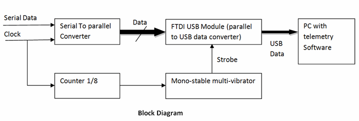
As it is seen in the block diagram above, I have used 1/8 counter for sending a write strobe to USB module and Serial To Parallel converter for writing parallel data to FTDI USB module.
This design gives me the flexibility to acquire data at different data rates. The only limiting factor is USB module which can transmit data of around 8mbps. Therefore using this design, I can acquire data from 1kbps to 8mbps.
Also data rate limitations are dependent upon the interface and not on the card design, hence I can achieve the maximum speed supported by the FTDI USB module which is 8mbps. Newer module supports even more higher data rate and one can simply start using newer module without changing much design of the card. I have used FTDI UM245R development module. It is a parallel to USB module and utilizes FIFO communication. Therefore, it is easier for the PC application to handle the data.
Another benefit of this design is that it is re-configurable which means that if any change occurs in data rate, frame format, frame size or frame sync, then the design of this card will not be changed. We can change these parameters or options through PC software.
Also, we can drive the circuit from the bus power of USB if the current requirements are below 500mA. Since we are not using any micro-controller or any other IC which requires more power, we can drive our circuit from USB bus power and because of that an additional need of external power supply is excluded and the card design becomes highly portable.
Circuit Diagram for the Card
Schematic diagram of the circuit is given below. I have used opto-coupler to decouple external system from our acquisition card whereas other functionality is the same as described in the description of block diagram.

This is text.
PC Software
A PC application can access the device in two ways; one is through the use of VCP driver and other is through D2XX drivers. In VCP, we configure the USB as virtual serial port. In virtual serial port mode, Data rate is 220Kbytes/sec whereas when D2XX drivers, the data rate is 1Mbytes/sec.
We are using .NET and C# to handle the USB data. In virtual serial port mode, the device just behaves like a serial port and we use the SerialPort Class of the .NET framework to access the data. If we want to use D2XX drivers, there is a wrapper provided by the FTDI to access USB port.
One major challenge in software design is to find the frame sync in the data bytes. Since frame sync can start from any bit position within a byte; we have to re-arrange the whole data to put the starting bit of frame sync at the starting bit of a byte. This orientation is necessary for real-time display and data processing. PC software description will be discussed in another article.
Conclusion
In this article, I have discussed the design of a digital data acquisition card and its advantages compared to another design. I am using this card in many of my projects and it is working absolutely fine.


 General
  News
News  Suggestion
  Question
  Bug
Bug  Answer
  Joke
Joke  Praise
  Rant
Rant  Admin
Admin 


